
Premium Silicon Wafers
Setting Tier-1 global standards for premium manufacturing with advanced wafer technology.
Next-Generation Silicon Wafers
210mm
Large-format N-Type monocrystalline wafers
Zero
Light-induced degradation (LID) for maximum lifespan
<130μm
Ultra-thin precision slicing technology
<130
210
>25
Cz
Zero
What is Silicon?
Silicon is the second most abundant element in the Earth's crust, primarily found in sand. However, for solar applications, it must be refined into extremely pure polysilicon (99.9999999% pure). This high-purity semiconductor material possesses the unique ability to convert sunlight into electricity through the photovoltaic effect.
What are Wafers?
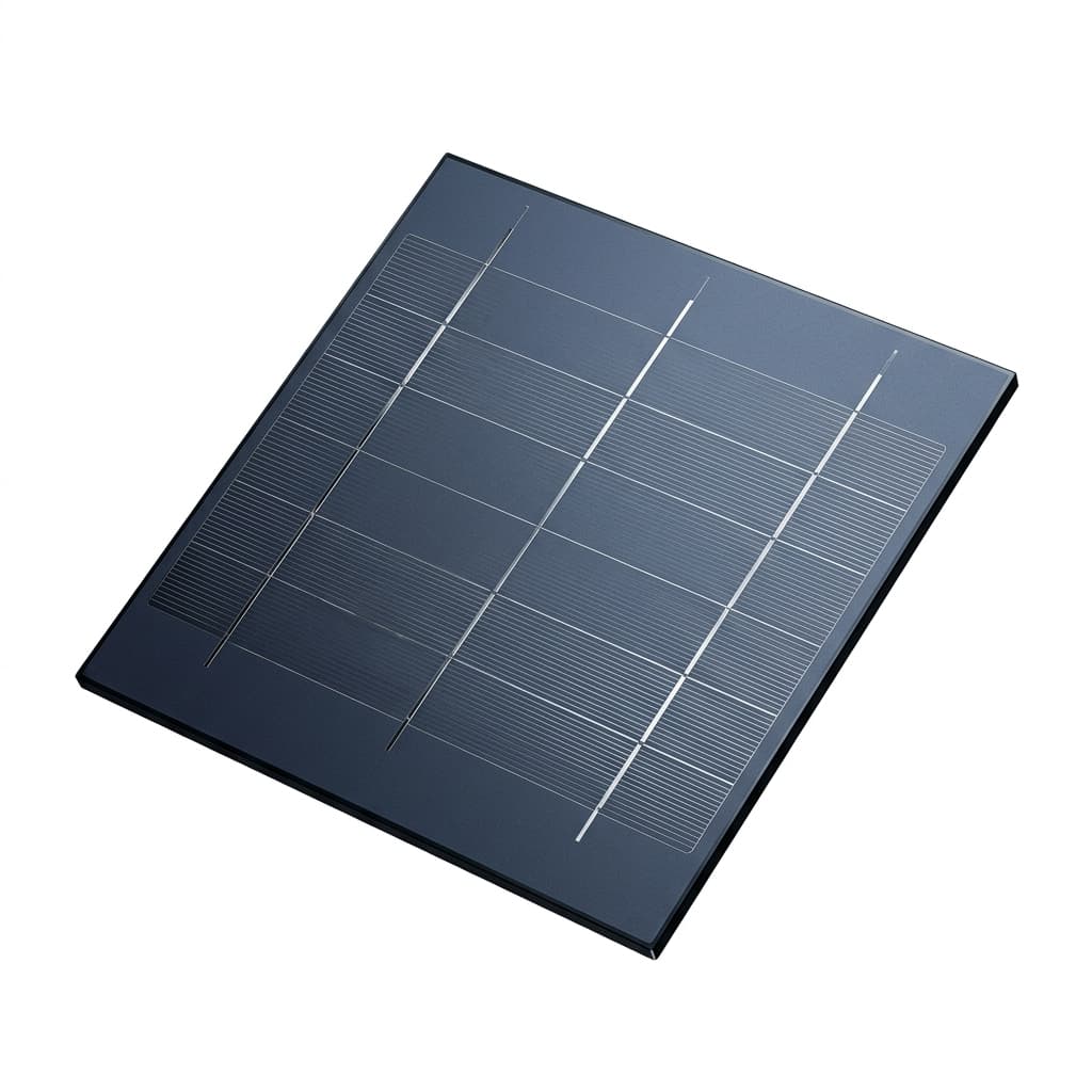
A silicon wafer is an ultra-thin (less than the thickness of a human hair) square slice of a single-crystal silicon block. It serves as the physical and electrical heart of a solar panel. Once cut, these wafers are processed into Solar Cells, which are then assembled into the solar panels that power homes.
The Manufacturing Timeline
Our state-of-the-art facility is designed to take premium imported polysilicon and transform it into world-class N-Type wafers through a rigorous, highly automated process.
Sourcing Premium Polysilicon
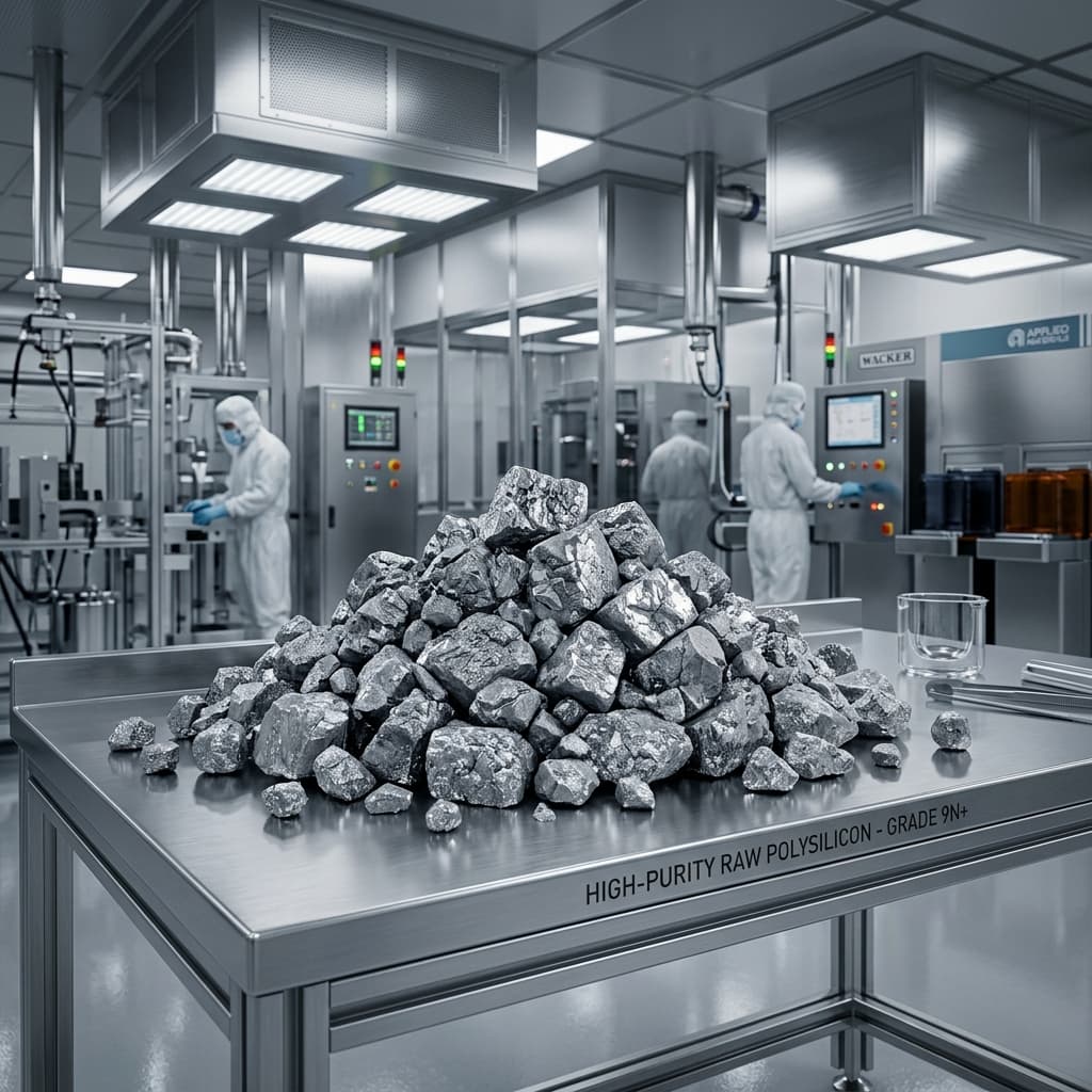
We begin by importing the highest grade (11N) electronic-grade polysilicon. This ultra-pure raw material is the critical foundation for high-efficiency N-Type solar cells.
Czochralski (Cz) Ingot Pulling
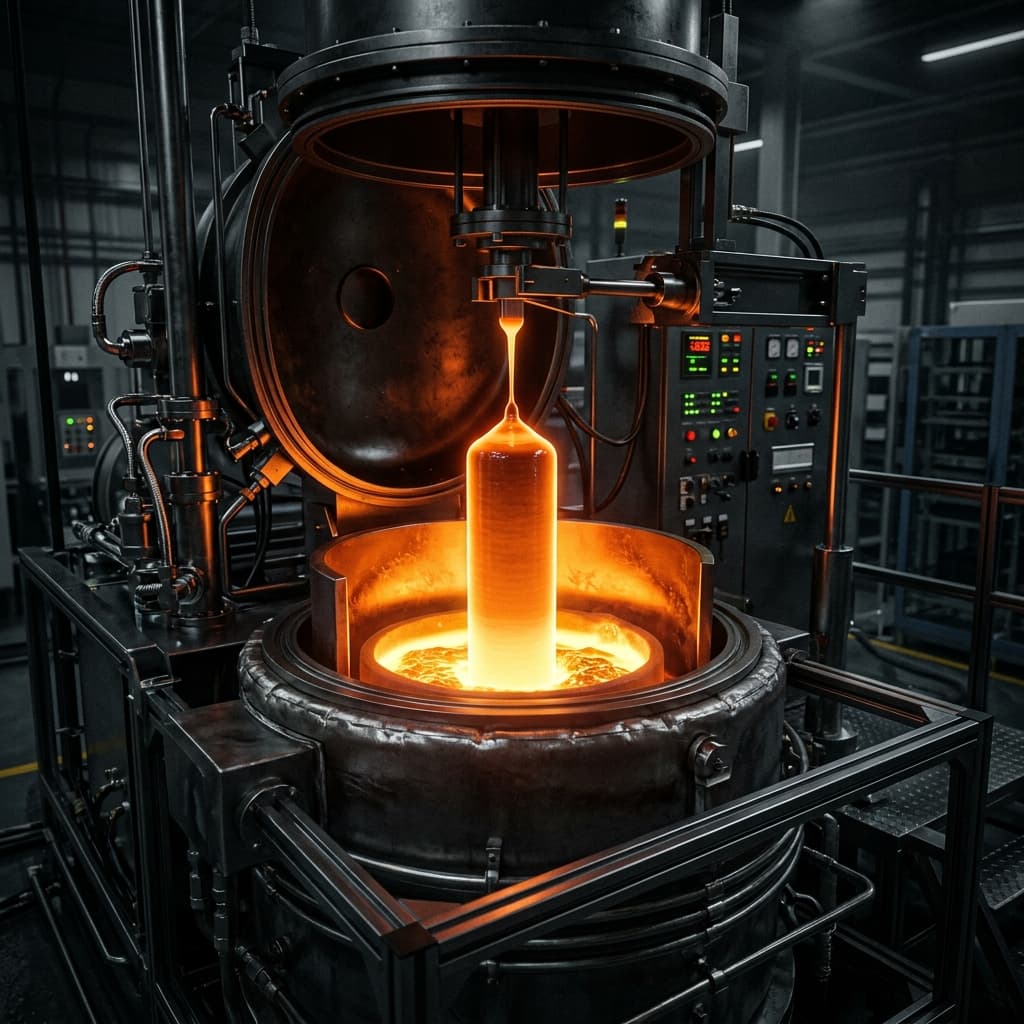
The polysilicon is melted in a quartz crucible at over 1,400°C. A seed crystal is introduced and slowly pulled upwards, growing into a massive, perfect single-crystal cylindrical ingot.
Squaring & Cropping
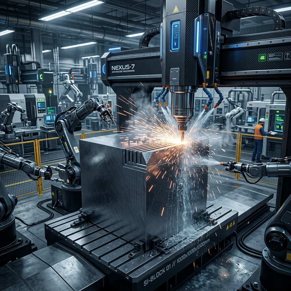
The cylindrical ingot is precisely cropped to remove uneven ends and then meticulously machined into a perfectly shaped square block, optimizing it for maximum surface area.
Diamond Wire Slicing
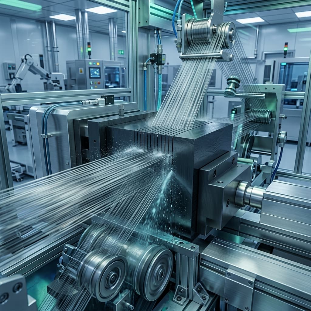
Using state-of-the-art diamond wire technology, the squared ingot is sliced into ultra-thin wafers (under 130μm). This minimizes kerf loss and maximizes yield.
Cleaning & Quality Assurance
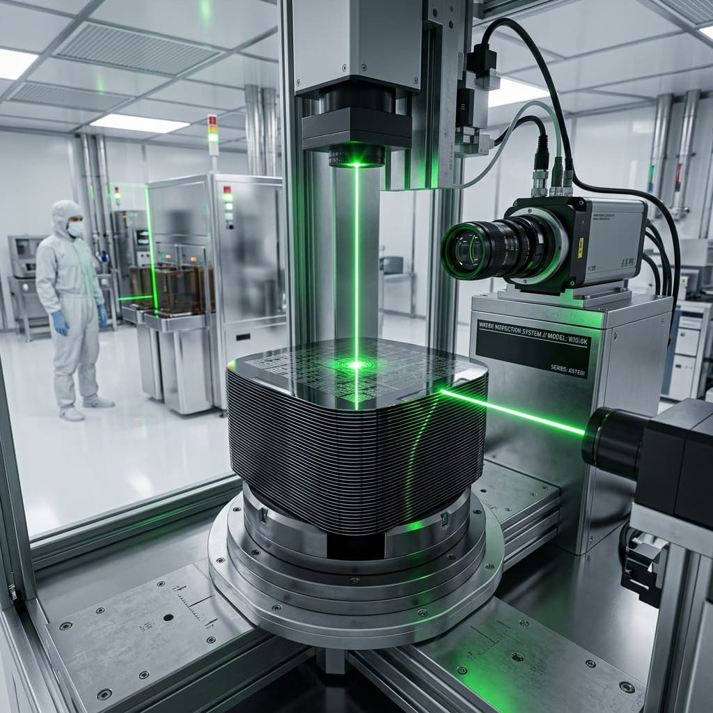
Each wafer undergoes rigorous chemical cleaning and automated optical inspection to detect micro-cracks or defects, ensuring a zero-defect standard before moving to cell production.